Full Complement Cylindrical Roller Bearing Cylinder Roller Bearing,Full Complement Cylindrical Roller Bearings,No Inner Ring Needle Bearing,Full Complement Needle Roller Bearing Changzhou Fangya bearing Co.,LTD , https://www.czfybearing.com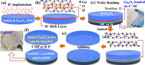
Research progress on heterogeneous integration of ultra-wide band gap semiconductors
[ Instrument Network Instrument R & D ] Researcher Ou Xin from Shanghai Institute of Microsystem and Information Technology, Chinese Academy of Sciences, and Professor Han Genquan from Professor Hao Yue of Xidian University have made new progress in the field of gallium oxide power devices. The research results were formally released at the 65th International Microelectronic Device Conference-International Electron Devices Meeting (IEDM) on December 10 in the form of an oral report: First Demonstration of Waferscale Heterogeneous Integration of Ga2O3 MOSFETs on SiC and Si Substrates by Ion-Cutting Process. This is the first paper published by China (including Hong Kong, Macao, and Taiwan) at the IEDM conference in the field of ultra-wide band gap semiconductors, indicating that China has also become one of the important innovative countries in the field of gallium oxide research.
As a third-generation wide bandgap semiconductor material, gallium oxide has the advantages of a wider band gap and higher breakdown field strength. Ga2O3 is one of the wide band gap semiconductor materials with the largest band gap. For high power and high frequency equipment, gallium oxide has great strategic significance and economic value. Its Baliga figure of merit is four and ten times that of GaN and SiC, respectively, providing a broader perspective for the development of future power devices. According to the market forecast of the Japanese authoritative economic research institution Fuji KeiZai, by 2025, the market share of gallium oxide in the entire third-generation semiconductor material is 27%.
However, due to the extremely low thermal conductivity of gallium oxide, the heat dissipation ability has become the biggest bottleneck of gallium oxide power device applications. Ou Xin's group and Han Genquan's group used the “universal ion knife†intelligent stripping and transfer technology to combine wafer-level β-Ga2O3 single crystal thin film (<400 nm) with highly thermally conductive Si and 4H-SiC substrate wafer level for the first time. Integrated and produced high-performance devices. The thickness non-uniformity of high-quality gallium oxide thin film is ± 1.8%, and the surface roughness of the thin film after optimization through chemical mechanical polishing reaches below 0.4nm. The electrical test of the device shows that the on-state current and the off-state current do not degrade significantly during the temperature rise of 300K to 500K. Compared with devices based on homogeneous gallium oxide substrates, the thermal stability has been significantly improved. SiC-based gallium oxide MOSFET devices When the temperature is 500K, the breakdown voltage can still exceed 600V.
Gallium oxide is undoubtedly a typical representative of ultra-wide bandgap semiconductor materials. The bandgap width can be close to 5eV. Today, the diamond material doping technology can not be broken today. This work has a milestone in the field of ultra-wide bandgap materials and power devices. important meaning. Firstly, heterogeneous integration provides a solution for the heat dissipation problem of Ga2O3 wafers, which is bound to promote the development of high-performance Ga2O3 device research; secondly, this research will provide high-quality high-thermal-conductivity substrate materials for the basic research and engineering of Ga2O3 in China, and promote Ga2O3 Large-scale applications in the field of high-power devices.